n. 4 – August 2022

EBL and FIB lithography to produce plasmonic single nanostructures or arrays on support

Written by Martina Elisena Recchia (ESR1)

Thanks to their optical properties, including the ability to confine light in spatial regions below the diffraction limit, plasmonic nanostructures have found important applications in many different fields.

Figure 1 Plasmonic nanostructures with various light management mechanisms. a) Localized Surface Plasmon Resonance (LSPR) of plasmonic nanoparticles. b) Surface Plasmon Polariton ( SPP) mode propagating on the surface of plasmonic arrays. c) Fabry-Pérot ( F–P) cavity mode generated by “metal–dielectric–metal” three-layer structures. d) Gap mode generated by adjacent metal particle-film and close packed particle–particle structures. e) Surface Lattice Resonances (SLR) mode generated by ordered plasmonic arrays. f) Fano resonance generated by plasmonic nanostructures with symmetry breaking or clusters of plasmonic nanoparticles. Reproduced with permission from Ref. [1] .

As reported in Figure 1 [1] nowadays it is possible to find a huge variety of plasmonic nanostructures that give rise to a plethora of phenomena due to their single or multiple resonances.

Thanks to the capability of supporting many types of plasmonic resonant modes and the possibility of simultaneously exciting them, metallic plasmonic single structures and arrays, built on supports, are exponentially gaining attention.

The fabrication of metallic plasmonic structure on substrates can be divided into two steps: template fabrication and metal deposition. The former procedure consists of using various nanofabrication techniques to form a basic pattern, while the second transforms the template into a metallic plasmonic array with the desired structure.

In the micro-fabrication industry environment, the most widely used technique to form an exposure pattern is the photolithography, due to the possibility of realizing simultaneously multiple devices, which uses photomask. It is limited in resolution by the diffraction limit of light, thus turning inadequate to obtain high-quality nanostructured features.

One group of emerging techniques which can overcome this limit are the direct writing lithography (DWL) such as Electron Beam Lithography (EBL) and Focused Ion-Beam (FIB) lithography.

In EBL systems [2] a highly focused and accelerated beam of electrons is scanned over a surface covered by a resist (the so-called e-beam resist), sensitive to electron radiation, to pattern features down to sub-10 nm. The e-beam can expose different areas and geometries of the substrates thanks to deflector coils or stage movement. Based on the type of resist used, the exposed areas become more or less soluble in organic solvents, enabling selective removal of either the exposed or non-exposed regions of the resist. Afterwards, a layer of metal is deposited on the obtained structure. With the removal of the remaining resist, covered also by the redundant metal, typically made with the lift-off method, and a final cleaning of the sample, the plasmonic metallic pattern is obtained (Figure2a ).

Figure 2 (a) Schematic overview of individual steps in the EBL fabrication process of plasmonic structures. (b) SEM image of a bowtie aperture with G = 11 nm, overlapped with field intensity enhancement profiles at its resonance wavelength. The scale bars are all 100 nm. Reproduced and adapted with permission from Ref. [3].

The primary advantage of electron beam lithography is that it is not limited by diffraction, thanks to the very small electron wavelength (typically less than 0.01 nm at 20 keV) and thus can write custom patterns with sub-10 nm resolution. Based on the system, the resolution is mostly limited by imperfections in the electron optics and electron backscattering from the substrate. Electron beam lithography systems expose resists one pixel at a time. For high throughput, it is desirable to have a large beam current. By increasing the beam current also the beam diameter increases which results in lowering the resolution. For this reason, typically EBL systems have a low throughput, favoring the resolution. As an example, in Figure2b is reported a Scanning Electron Microscopy (SEM) image of one bowtie plasmonic aperture produced by Huang et al. [3], characterized by gap size down to 11 nm and silver film thickness up to 150 nm, fabricated on a silicon nitride membrane. One the SEM image is overlapped the mode profile for the 11 nm gap aperture at its resonance wavelength, obtained using three-dimensional (3-D) finite-difference time-domain (FDTD) simulations.

The focused ion beam (FIB) lithography system [4] follows a similar approach to EBL but it uses high-mass ions, such as gallium ions, as the energy carriers instead of electrons. It is more straightforward compared to the EBL because it consists of just two steps: the deposition of the metal layer and the exposure to the focused ion beam, to pattern features (Figure3a) again down to sub-10 nm. FIB patterning is an inherently destructive process, as the bombardment of a surface with ions causes atomic sputtering from the surface.

For instance, Figure3b shows the results obtained by Chen et al. [5] in fabricating Au nanoparticle dimers with different shapes using the He+-FIB lithography technique.

Figure 3 : (a) Schematic overview of individual steps in the FIB lithography fabrication process of plasmonic structures. (b) High-resolution electron micrographs of single nanodimer of (from left to right) heart-shaped, bowtie-shaped, disk-shaped nanoparticle dimer. Scale bars: 100 nm. Reproduced and adapted with permission from Ref. [5].

Both of the above mentioned systems could be integrated in an Scanning Electron Microscope which allows a live view of the writing process (see Figure4).

Figure 4 (a) PIONEER Two from RAITH nanofabrication, Electron Beam Lithography (EBL) system combined with an analytical Scanning Electron Microscope (SEM) [6]. (b) Hitachi Ethos FIB-SEM (Focused Ion and Electron Beam System Ethos NX5000 Series) from HITACHI [7].
Figure 5 TEM bright field micrographs of 140-nm EBL and FIB antennas. Reproduced and adapted with permission from Ref.[8].

Horak et al. [8] proposed a comparative study of plasmonic antennas fabricated by EBL an FIB lithography. They studied four individual disc-shaped gold plasmonic antennas characterized by a designed diameter parameter of 120 nm and 140 nm (see Figure5 ) and designed height of 25nm. They characterized the produced antennas in depth, studying their three-dimensional (3D) morphology and LPR intensity peak and analyzing their chemical composition with the possible contaminations. For this work, the results showed that the EBL antennas had a better quality. They had rather homogeneous thickness profile with smooth thickness fluctuation, and sharper edges. The plasmonic response of the antennas fabricated by EBL turned out to be considerably stronger and slightly better localized than the antennas fabricated by FIB lithography. Moreover, the EBL antennas resulted in a less contaminated structures, since in FIB antennas both organic and inorganic contamination were present together with implanted ions from the focused beam.

In general, both particle fabrication techniques have their disadvantages. In EBL, the final structures can be contaminated by the residual resist or solvents and the lift-off can exert a pronounced mechanical force that can damage the fabricated structure or even the substrate. In FIB, chemicals are not involved in the process but the ions in the milling beam and atoms sputtered from the metal and substrate can still contaminate the fabricated structures. Moreover, although large area mechanical effects are not present, local damages could be caused by the focused ion beam. Considering the resolution, the helium ion beam nanofabrication method developed in recent years has higher resolution (around 5 nm) than electron beam exposure [9]. The time and potential risks of the fabrication process should be taken into account as well, while choosing one of the two presented methods. FIB preparation is more straightforward and simpler because no chemistry is used, thus it is faster for individual antennas or small series of antennas. EBL preparation provides generally antennas with higher quality, but the lithographic process induces potential risks of damaging the sample as the wet chemistry is used. EBL is more time consuming than FIB if a small number of antennas is prepared, but much faster if a large array of antennas is fabricated. In fact, even if EBL consists of more steps, the single exposition is considerably faster than for FIB.

OPTO NANO – A duet of Science and Contemporary Dance

Written by Nicole Slesiona (ESR3)

“Movement is the essence of life.” A description by biology professor Bernd Heinrich from the university of Vermont that summarizes the definition of what makes us and everything around us alive: Movement. Indeed, the training network is dedicated to developing new technologies that will help future generations of scientists to unveil a more detailed understanding of how electromagnetic waves, inorganic nanomaterials, and molecules interact with and influence each other. With the tools of coherent nonlinear microscopy, coherent ultrafast spectroscopy, or nano-plasmonics at the heart of their labour, our researchers hope to contribute to next-generation imaging modalities.

Three of our ESRs, usually focussed on analysing the electronic response of metallic or semiconducting nanostructures to electromagnetic waves, were invited to change their perspective on their scientific and oftentimes highly conceptual work and translate their science into choreographed movement. This invitation stems from a collaboration between Professor Paola Borri, head of the Quantum Optoelectronics and Biophotonics group at Cardiff University and coordinator of the MUSIQ consortium, and Jack Philp, a choreographer who dedicated his work to connect biophysics, live performance, and digital technology, to create inspiring and thought-inducing choreographies that translate biophysics into movement. Prof Borri is herself an amateur contemporary dancer and met Jack Philp in 2018 while attending one of his community classes in Cardiff. Over a chat on the way home, they realised their common interest and passion for science and dance and decided to collaborate on creating a new art-science project.  Prof. Borri invited Jack Philp to visit her lab at Cardiff University and they were both thrilled by the opportunity of translating some of Prof. Borri’s research work into an art form through contemporary dance. They started looking for art-science funding opportunities via a few routes. Prof. Borri helped raising an initial sponsorship from Cardiff University, for a creation phase in June 2019, where OPTO NANO was born. Jack Philp then secured substantial funding from the Arts Council of Wales for a Research and Development phase in November 2019 and a production phase in 2021, while Prof. Borri helped raising side sponsorships from the UK Engineering and Physical Sciences Research Council (via the IBIN network), and the European consortium MUSIQ.

Figure 6 Photo of the dancers Fern Grimbley, Chandenie Gobardhan, Rose Lewis, Chelsea Gordon, and Gaia Cicolani.

Martina Recchia (ESR1), Vikramdeep Singh (ESR2) and Nicole Slesiona (ESR3) were guided by Jack over the course of three days to get insight into the thought process contemporary dancers go through when translating concepts of science into movement. On the first day, the ESRs were allowed to observe a highly skilled and diverse team of dancers working on expressing the movement of water molecules into a highly dynamic and fluid dance. This built the basis for both, the researchers and the dancers, to form what would become a bridge of understanding between the two seemingly opposing disciplines of arts and science. “I was astonished with Jack’s ability to transcribe his work in a way that we could immediately pick up on and work with. In return he would translate our sometimes admittedly complicated scientific language into something that the dancers would instantly be able grasp as well”, Nicole commented after the training. After being sent home with a piece of homework to think about where movement plays a vital role in their project, our ESRs returned the next day to develop a concept the dancers could work with under Jacks guidance. Martina commented on her thought process with Jacks guidance: “In my project we excite lipid molecules using two laser beams. These causes the molecules to vibrate coherently and, consequently, to emit light. The introduction of nanoparticles makes the emitted light stronger and easier to detect. After having watched Jack and the dancers during our first day and having learnt the basic principle of translating science into movement, my idea was to have a choreography divided in three sections. A first part in which each dancer improvises disorganised movements. Then a sudden change of music and / or lights to indicate excitation by a laser, with the dancers now performing the same movements in unison. The final part represents what would happen with a nanoparticle in vicinity to the molecules: the movements become amplified, clearer and more defined”.

Figure 7 Martina Recchia and Vikramdeep Singh working with the dancers.

The dancers worked in three groups with Martina, Vikram and Nicole individually to then return to everyone with a first draft for a choreography the dancers would later be able to build upon. The third day was spent to allow feedback between the dancers and the ESRs to refine the established ideas, ask questions, and to form a deeper appreciation of both sides for each other and how they, respectively, contribute to society. From here, Jack took his project to critically acclaimed composer R. Seiliog to produce a unique electronic sound score specifically for this choreography. With light design by Barnaby Booth and Joshua Harrietteas the final brush stroke, the collaboration culminates in a symphony of movement, science, light, and colour.

For further information, see: https://www.jackphilpdance.co.uk/opto-nano-tour

About the Authors

The MUSIQ Innovation Newletter n. 4 was written by two of the Early Stage Researchers (ESRs) working on individual projects as part of the MUSIQ project.

Martina Elisena Recchia (ESR1)
Martina is hosted at Cardiff University, School of Biosciences, in the UK. Her research project focuses on understanding and controlling lipid membranes at the nanoscale through label-free coherent nonlinear optics at membrane-nanoparticle interfaces.

Nicole Slesiona (ESR3)
Nicole is hosted at the School of Biosciences at Cardiff University working on Four-Wave-Mixing microscopy for visualising
endocytic pathways of mammalian cell line systems using gold nanoparticles.

References

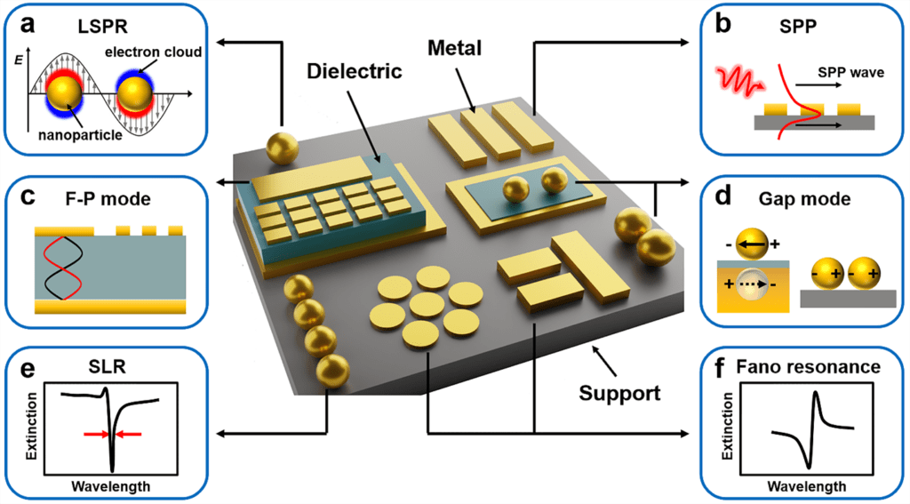
[1] Yang, K., Yao, X., Liu, B., & Ren, B. (2021). Metallic plasmonic array structures: Principles, fabrications, properties, and applications. Advanced Materials, 33(50), 2007988.

[2] Vieu, C., Carcenac, F., Pepin, A., Chen, Y., Mejias, M., Lebib, A., … & Launois, H. (2000). Electron beam lithography: resolution limits and applications. Applied surface science, 164(1-4), 111-117.

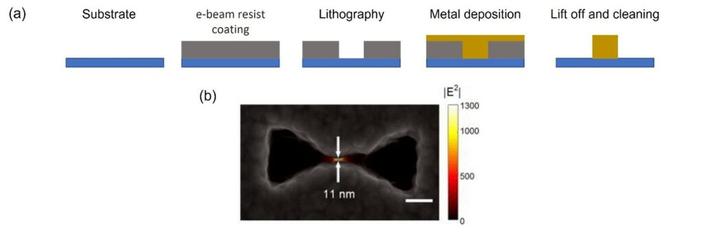
[3] Huang, I. C., Holzgrafe, J., Jensen, R. A., Choy, J. T., Bawendi, M. G., & Lončar, M. (2016). 10 nm gap bowtie plasmonic apertures fabricated by modified lift-off process. Applied Physics Letters, 109(13), 133105.

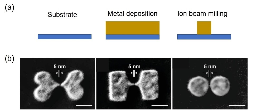
[4] Joshi-Imre, A., & Bauerdick, S. (2014). Direct-write ion beam lithography. Journal of Nanotechnology, 2014.

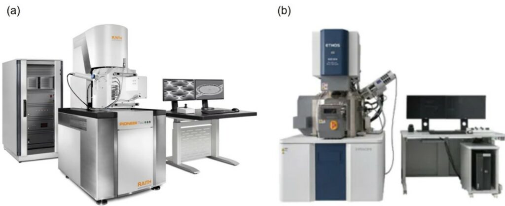
[5] RAITH nanofabrication, accessed 18 March 2022, https://raith.com/product/pioneer-two/

[6] Hitachi, accessed 18 March 2022, https://www.hitachi-hightech.com/global/product_detail/?pn=em-nx5000

[7] Chen, Y., Hu, Y., Zhao, J., Deng, Y., Wang, Z., Cheng, X., … & Duan, H. (2020). Topology optimization‐based inverse design of plasmonic nanodimer with maximum near‐field enhancement. Advanced Functional Materials, 30(23), 2000642.

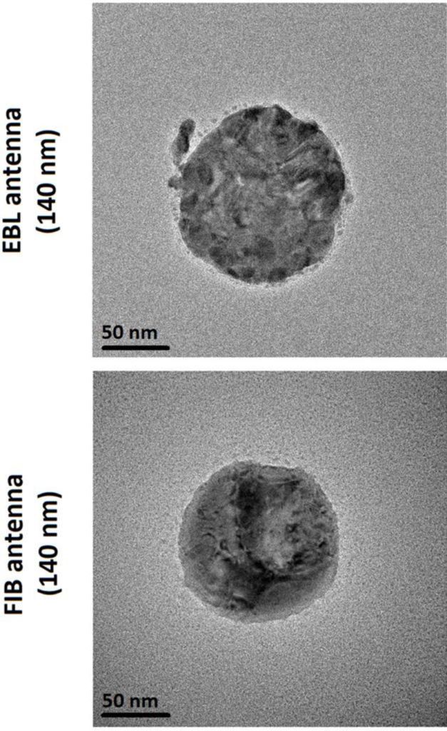
[8] Horák, M., Bukvišová, K., Švarc, V., Jaskowiec, J., Křápek, V., & Šikola, T. (2018). Comparative study of plasmonic antennas fabricated by electron beam and focused ion beam lithography. Scientific Reports, 8(1), 1-8.

[9] Klingner, N., Hlawacek, G., Mazarov, P., Pilz, W., Meyer, F., & Bischoff, L. (2020). Imaging and milling resolution of light ion beams from helium ion microscopy and FIBs driven by liquid metal alloy ion sources. Beilstein Journal of Nanotechnology, 11(1), 1742-1749.